 SATVARTH
Your Tech Partner for Scalable, Smart Solutions
At Satvarth, we blend innovation with functionality to craft seamless digital experiences across platforms. Our full-stack team turns ideas into high-performing solutions.
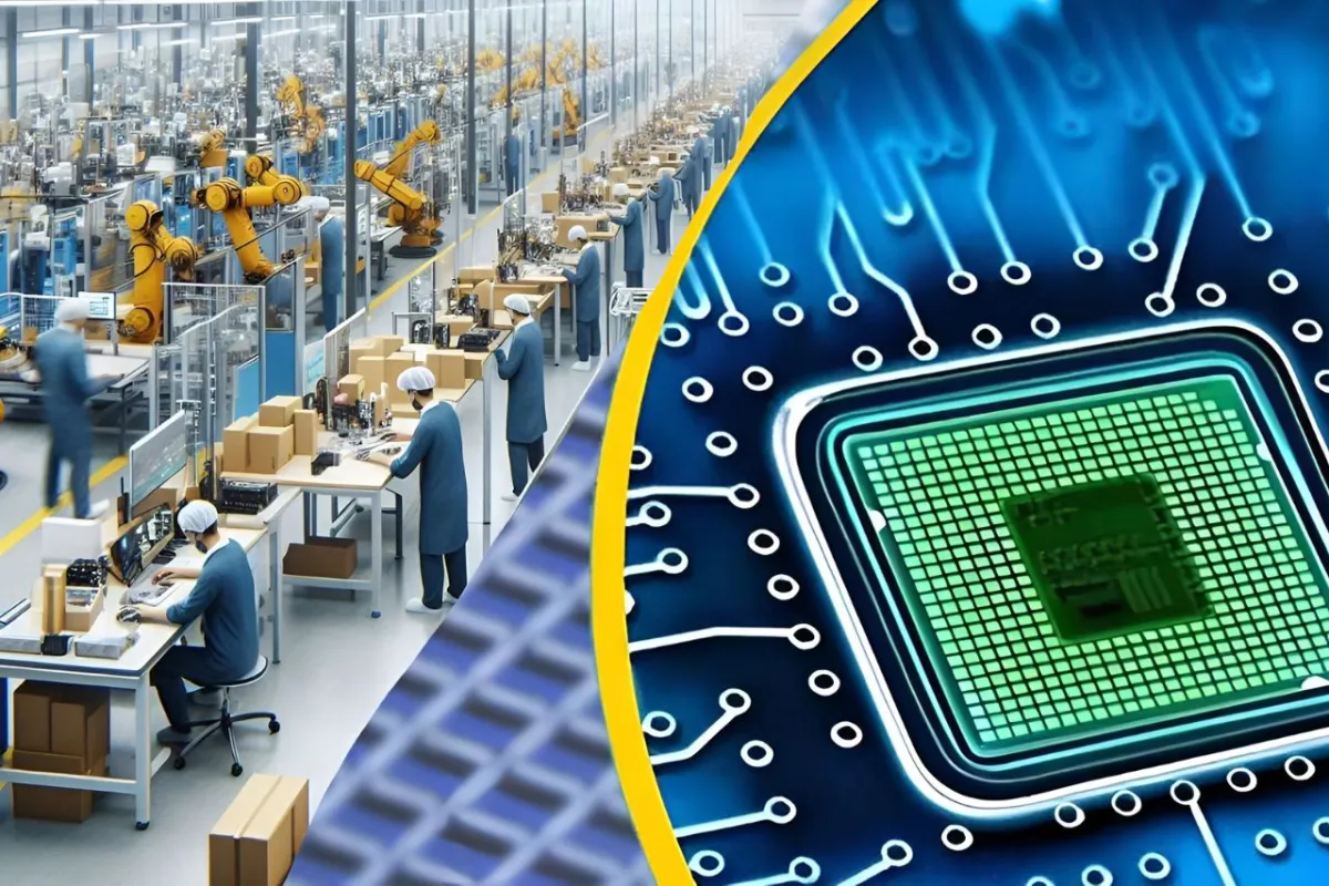
Semiconductor Mission 2.0

India is actively working to build strong talent in the semiconductor sector through the Chips to Startups (C2S) program, launched under the India Semiconductor Mission 2.0 (ISM). According to the Union Minister for Information and Broadcasting, Electronics and Information Technology, and Railways, the country has made significant progress in just four years toward its long-term goal of training 85,000 engineers in semiconductor design over the next decade. This initiative aims to strengthen India’s capabilities in chip design and support the growth of the domestic semiconductor ecosystem.
World-class tools now in academic institutions

The minister also shared that Electronic Design Automation (EDA) tools from leading companies such as Synopsys, Cadence, Siemens, Renesas, Ansys, and AMD are now available in 315 academic institutions across India. These advanced tools give students hands-on experience in designing semiconductor chips. The designs created by students are then fabricated and tested at the Semiconductor Laboratory (SCL) in Mohali, according to an official release.
Through this practical approach, students get exposure to the entire chip development cycle, starting from design and fabrication to packaging and testing. The initiative has grown into the largest open-access EDA program in the world, with users already recording over 1.85 crore hours of EDA tool usage.
Through this practical approach, students get exposure to the entire chip development cycle, starting from design and fabrication to packaging and testing. The initiative has grown into the largest open-access EDA program in the world, with users already recording over 1.85 crore hours of EDA tool usage.
Students across India join the semiconductor journey

Students from across India—from Assam to Gujarat and from Kashmir to Kanyakumari—are now actively taking part in semiconductor design activities. This widespread participation is a major milestone for the country, as it helps build a strong talent base that will support India’s technological growth and strengthen its journey toward self-reliance in the semiconductor sector.
Huge employment opportunities in a growing industry
The minister also highlighted that the global semiconductor market is expected to grow significantly—from its current value of $800–900 billion to nearly $2 trillion in the coming years. This rapid expansion will create a worldwide demand for around 2 million skilled professionals, opening up major job opportunities for Indian youth in areas such as chip design, fabrication, packaging, and testing.
Expansion under India Semiconductor Mission 2.0

To further strengthen this effort, the government has announced the India Semiconductor Mission 2.0, which will expand the program’s reach from 315 academic institutions to 500 educational institutions across the country. This expansion aims to create a steady pipeline of skilled professionals who can support the semiconductor industry in every state, while also helping India build a strong and self-sustaining semiconductor ecosystem.
Commitment to a global semiconductor hub
The minister explained that the Government of India plans to build a strong semiconductor industry by focusing on three key pillars: talent development, infrastructure development, and partnerships with industry organizations. Through these initiatives, India aims to become a major global hub for semiconductor design and manufacturing, creating thousands of new job opportunities and strengthening the country’s position as a leader in global technology.
(401)